Organic photovoltaics, solar energy devices based on organic semiconductors, have so far achieved very promising results in experimental settings, both in terms of efficiency and stability. However, engineers have not yet devised reliable strategies to fabricate these devices on a large-scale at a reasonable cost.
Researchers at Wuhan University in China have recently identified an approach that could facilitate the rapid fabrication of photoactive layers for organic solar cells, without compromising the cells’ efficiency and stability. Their proposed strategy, introduced in a paper published in Nature Energy, is based on sequential deposition, a method often used to deposit organic semiconductors and perovskite films on substrates.
“To realize the commercialization of organic photovoltaics (OPVs), the golden triangle of power conversion efficiency (PCE), stability, and cost should be considered simultaneously,” Jie Min, one of the researchers who carried out the study, told TechXplore.
“At present most researchers are focusing on these three parameters. In the energy industry, however, people are paying more attention to the Levelized cost of energy or electricity (LCOE), which is more relevant to end customers with production incentives, its calculation involves many local techno-economic assumptions including life cycle analysis, module operating temperature and high processing throughput, etc.”
To assess organic solar cells, Min and his colleagues wished to reach beyond the so-called “golden triangle” of efficiency, stability and cost. Specifically, they wanted to focus on the LCOE, which measures the average net present cost of electricity generation for a specific generator or energy device over the course of its lifetime.
The researchers feel that this measure is particularly relevant for the current state of OPV development, due to the advancements they could bring in terms of efficiency and stability. More specifically, the large-scale commercial development of OPVs will only be possible once their throughput and module yield significantly increase, which will in turn reduce the overall cost of solar cells.
“For instance, increasing the throughput from 1.44 to 3.0 m2 min-1 reduces the manufacturing cost by 20%, as predicted in one of our previous reports,” Min explained. “This analysis provides a prerequisite for us to find approaches to solve the high throughput issue in the progress of module fabrication. And we think high-throughput factor is as important as the three parameters of the ‘golden triangle.'”
In some of their previous papers, Min and his colleagues showed that OPV systems that exhibit high efficiencies can only be routinely blade-coated and slot-die coated at linear speeds of 0.3–1.5 m min−1. Unfortunately, these rates are still significantly lower than those attained by silver grid electrode processes (>20 m min−1) and interfacial layers printing processes (>10 m min−1).
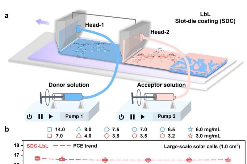
“The key objective of our study was to identify effective strategies to solve the high-throughput issue of photoactive layers,” Min said. “For our happiness, we were also able to identify a viable layer-by-layer (LbL) processing technique.”
Min and his colleagues were able to create a photoactive layer of OPVs with a high coating speed, using an LbL processing strategy. This strategy entails the sequential deposition of donor and acceptor layers, rather than the mixture of donor and acceptor materials to create a so-called bulk-heterojunction, which is what traditional deposition methods are based on.
“In our previous works, we found that this LbL method can not only improve device efficiency and stability, but also can overcome the scaling lag of device or module efficiency,” Min said. “Other studies also showed that this LbL approach can improve the exciton diffusion length in devices and overcome the molecular weight issue resulting from suitable vertical phase morphologies fabricated by LbL methods.”
The recent findings gathered by Min and his colleagues confirm some of their previous findings, by showing that LbL processing methods are robust and less dependent on general film-forming conditions than methods based on the donor:acceptor bulk-heterojunction. Notably, the processing strategy they identified is also applicable to non-halogenated solvents and works in conditions marked by high humidity.
“Our work shows that we should not only focus on the golden triangle of power conversion efficiency (PCE), stability, and cost, but also need to pay more attention to the important factors (e.g. high throughput), which also determine the possible applications of OPVs,” Min said. “In addition, I think our work is a good start in shifting our focus from the ‘golden triangle’ to the LCOE, especially for materials scientists and engineers.”
As part of their recent study, the researchers used the LbL processing technique they identify to create a series of photoactive layers for OPV systems, namely PM6:Y6, PM6:N3, PM6-Ir1:Y6, PM1:Y6 and PTQ10:Y6. However, it could also be applied to the fabrication of other non-fullerene photovoltaic systems.
“Our work represents a step towards the scalable, cost-effective manufacturing of organic photovoltaics with both high performance and high throughput,” Min added. “My future research plan will focus on two goals: one is to find an ideal material system, which possesses high efficiency, excellent stability, low cost of material synthesis and processability of high-speed coating, and the other is to construct a commercially available device architecture.”

