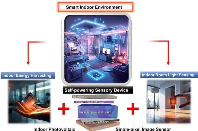
Organic-based optoelectronic technology is increasingly recognized as an energy-efficient solution for low-power indoor electronics and wireless IoT sensors. This is largely due to its superior flexibility and light weight compared to conventional silicon-based devices. Notably, organic photovoltaic cells (OPVs) and organic photodetectors (OPDs) are leading examples in this field.
OPVs have the remarkable ability to absorb energy and generate electricity even under very low light conditions, while OPDs are capable of capturing images. However, despite their potential, the development of these devices has thus far been conducted independently. As a result, they have not yet reached the level of efficiency necessary to be considered practical for next-generation, miniaturized devices.
A Korea Institute of Science and Technology (KIST) research team, led by Dr. Min-Chul Park and Dr. Do Kyung Hwang of the Center for Opto-Electronic Materials and Devices, Prof. Jae Won Shim and Prof. Tae Geun Kim of the School of Electrical Engineering at Korea University, Prof. JaeHong Park of the Department of Chemistry and Nanoscience at Ewha Womans University, have now developed an organic-based optoelectronic device.
The work is published in the journal Advanced Materials.
This innovative device not only integrates the functionalities of OPVs and organic OPDs but also visualizes images in applications requiring low-light conditions, thereby enhancing energy efficiency in indoor environments.
By advancing the organic semiconductor layer into a multicomponent structure, the research team has enhanced the device’s performance. In indoor environments, it achieves an impressive photoelectric conversion efficiency exceeding 32%, along with a linear dynamic range surpassing 130 dB. This significant improvement in contrast ratio, especially in low-light conditions, allows for a much clearer image than conventional silicon devices, which typically offer a linear dynamic range of 100 dB.
The collaborative research team made further strides by successfully applying single-pixel image sensing. This image sensing system captures ambient light, transforms it into electrical energy, and utilize this energy to acquire images.
In contrast to the previous need for specialized cameras in low-light conditions, the newly developed photodetector, featuring a multi-component semiconductor layer, offers a versatile platform. It can function not only as a conventional camera but also as a decorative element on windows or walls, providing sufficient resolution to discern shapes and movements of objects.
Dr. Min-chul Park from KIST highlighted the versatility of this technology, noting, “While primarily functioning as an energy harvester, it can also be applied to detect movement and recognize motion patterns in environments without light.”
He stated, “This holds great promise not only for human-computer interaction (HCI) research but also in various industrial sectors, including smart indoor environments.”

