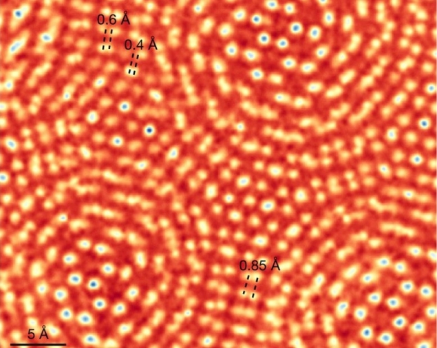
A new electron microscopy technique that achieves far better resolution than ever before, while also minimizing potential electron damage to the sample, has been unveiled by researchers in the US. The team presented images of the 2D material molybdenum sulphide that show unprecedented atomic-level detail, and they are confident that the technique could also be exploited in a range of applications where traditional electron microscopy has proved difficult.
Electron microscopes are valued for their increased resolution over visible light microscopes, thanks to the much smaller wavelength of electrons relative to photons. However, the resolution of these instruments is constrained by small aberrations in electron lenses, which limit the size of the aperture and make it difficult to focus the electron beam. Electron microscopists have so far achieved resolutions of around 0.5 Å (0.05 nm) in bulk materials – generally good enough to see individual atoms – by combining sophisticated and expensive aberration-correctors with shorter-wavelength, higher-flux electron beams that increase the signal-to-noise ratio.
Damage limitation
However, these shorter-wavelength, higher-energy electrons can do significant damage to samples, especially at high electron fluxes. “There are two damage mechanisms from electrons,” explains David Muller of Cornell University in New York. “One of them is that you ionize the sample and you kick electrons off. The other is that the electron transfers so much momentum to the nucleus that it kicks it off its lattice site and breaks bonds. The lower your beam energy the less you’re going to knock things around.”
These damage mechanisms have prevented the attainment of sub-angstrom resolutions in delicate samples such as 2D materials, which can rapidly be obliterated by a powerful electron beam: “If I have a 2D material and I knock off one atom every second, I’m going to notice almost immediately that it’s looking like Swiss cheese,” says Muller.
Muller and colleagues solved the problem by exploiting a technique called ptychography, which was first conceived for X-ray crystallography almost 50 years ago but in principle is equally applicable to imaging with electrons. The idea is to record the exact diffraction pattern built up on the detector from every point in the sample, and to study how this changes across the sample. From this information, it is possible to reconstruct the phase of the matter wave diffracted by the sample and to work out the shape of the diffracting object – in other words, the pattern of atoms.
As the technique not only records the beam intensity, but also uses it to reconstruct the underlying quantum wavefunction, it can extract much more information per electron – and so potentially requires far fewer electrons. But its use in electron microscopy has so far been hampered by the formidable requirements placed on the detector. This is because ptychography requires the phase of the wavefunction to be measured equally precisely in both dark and light spots, but in electron diffraction experiments the high-angle diffraction peaks are extremely dim compared to the signal from the main beam.
To address this problem, Muller and colleagues have developed a detector capable of recording single electrons, even though some pixels are subjected to an electron flux a million times greater than others. “Imagine I had a camera, and I took a picture of you and the Sun shining from behind you,” says Muller. “Our detector would be able to image all the sunspots on the surface of the Sun and all the details of your face in the shadow.” This new instrument, which the scientists have dubbed the electron microscope pixel array detector (EMPAD), allowed them to perform full electron ptychography for the first time.
The researchers demonstrated their approach by imaging the 2D material molybdenum disulphide. Despite using electrons of only 80 keV – less than half the 200 keV often used to image bulk samples – the researchers achieved record-breaking resolution of 0.39 Å. They were able to clearly discern features that were unclear in images produced using other techniques, such as a sulphur monovacancy – a random defect in which one of two sulphur atoms in the MoS2 lattice structure is missing but the other is still present.
The researchers are now looking at other types of systems, such as biological samples. “Biological materials are extremely sensitive to radiation,” says Muller, “so the resolution of biological systems in limited by the number of electrons you can put on the sample.” They are also studying tiny strains in catalyst nanoparticles, which are crucial for their chemical activity.
John Rodenburg of the University of Sheffield, one of the inventors of electron ptychography, is impressed. “Many years ago we showed that if you had a bad electron lens, you could improve on it many times. This paper is the first to show that you can way surpass even a good electron lens,” he says.
Rodenburg believes the real potential of the work is in 3D imaging. “The phase is linear as you put more atoms on top of one another,” he explains. “That gives you the possibility of getting the three-dimensional structure of a material out, and that’s what X-ray ptychography is mainly used for.”

